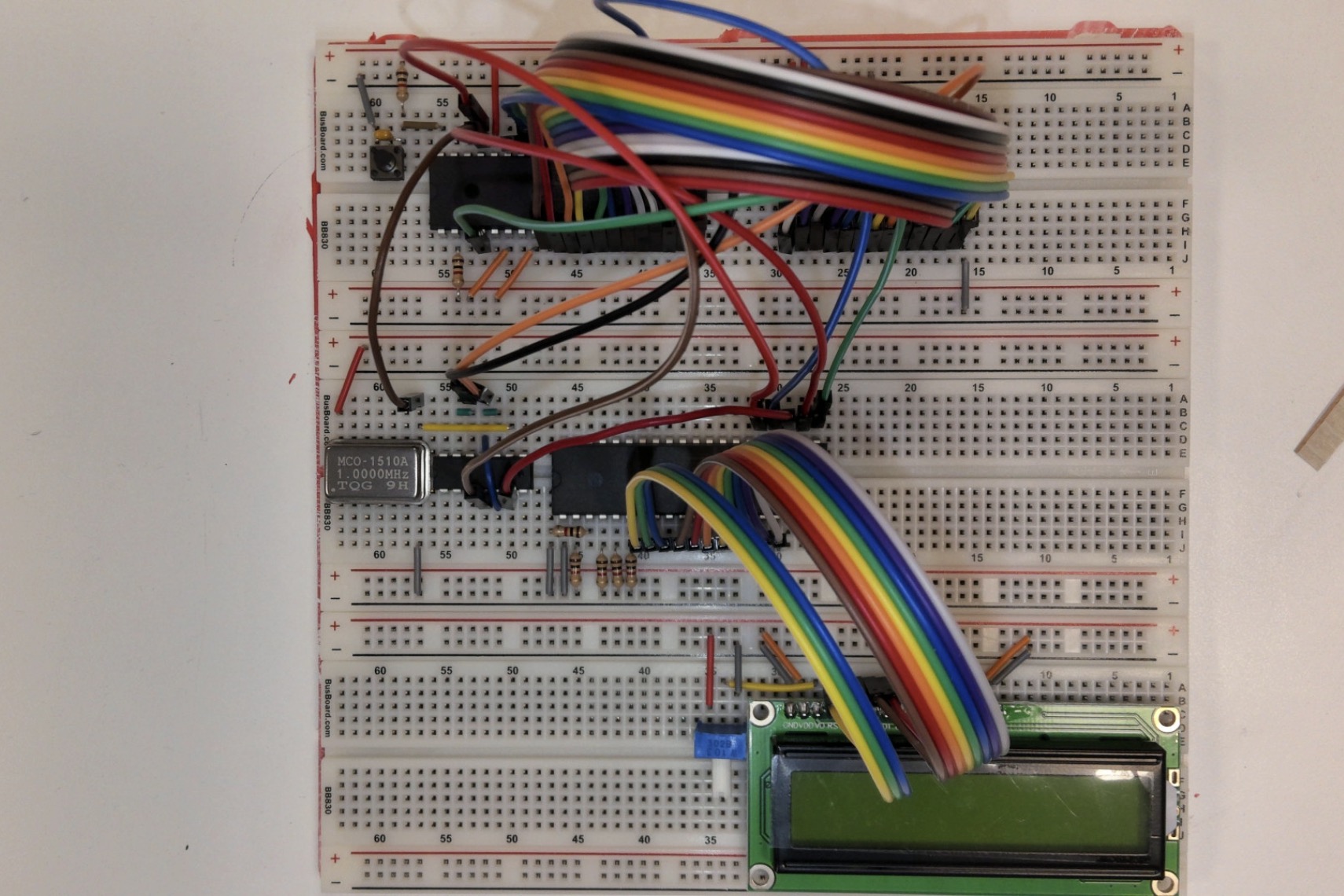
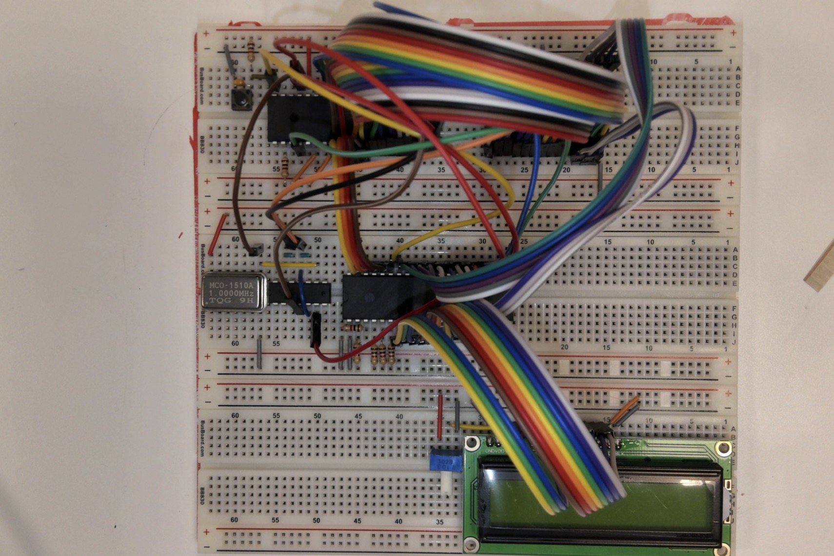
6502 Step-by-step-guide
This guide will walk you through how to assemble your 6502 from scratch! At the end of the guide, you will have printed the message "Hello World!" on a screen using only the 6502 CPU.
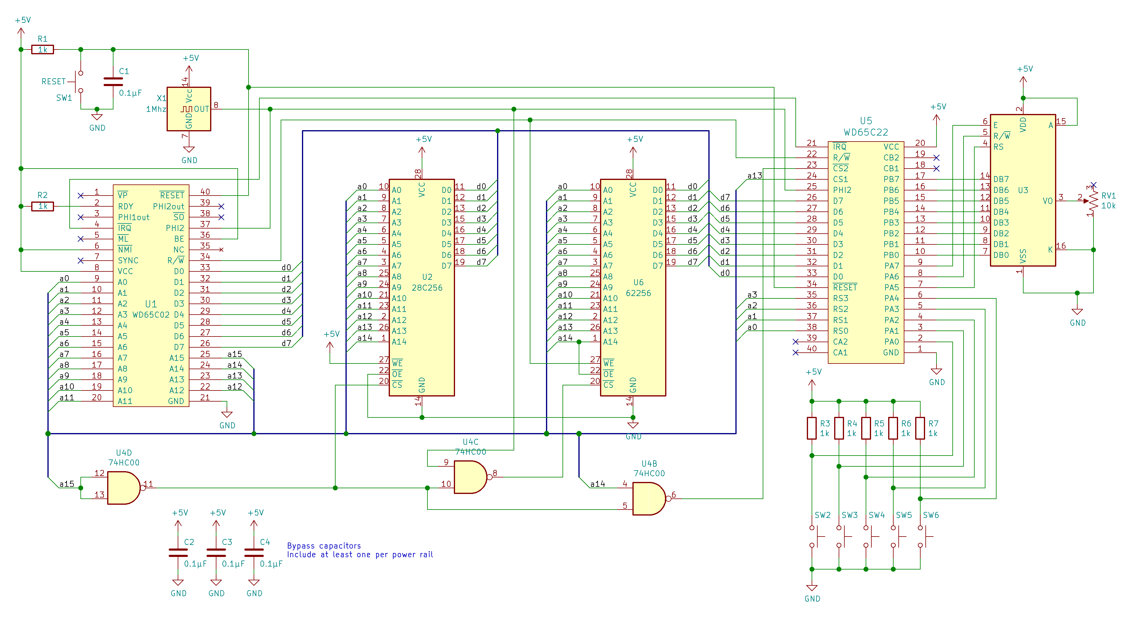
To build this CPU, you will need to reference this schematic from Ben Eater which showas the completed CPU: https://eater.net/schematics/6502.png
Each IC is labelled on the schematic, however as a reminder the WD56C02 is the 6502, the 28C256 is the EEPROM, the WD65C22 is the versatile interface adapter (VIA), and the IC labelled U3 is the screen. Note that pin layouts on schematic diagrams do not always follow the physical layout of the IC so make sure you double check the schematic diagrams for the ICs using the data sheets provided by Ben Eater:
Connect EEPROM to 6502
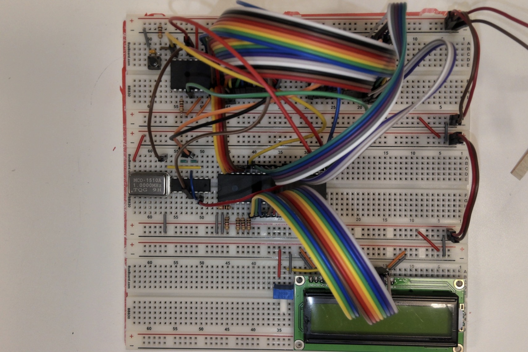
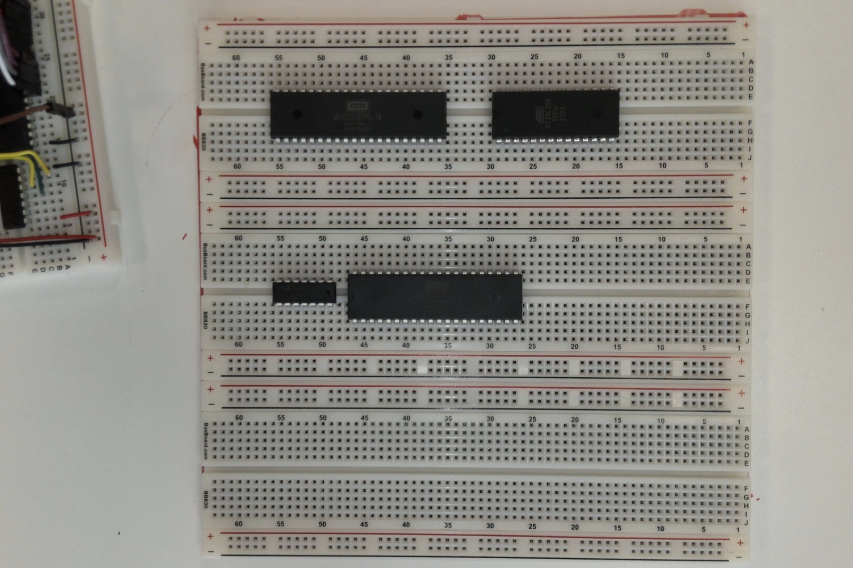
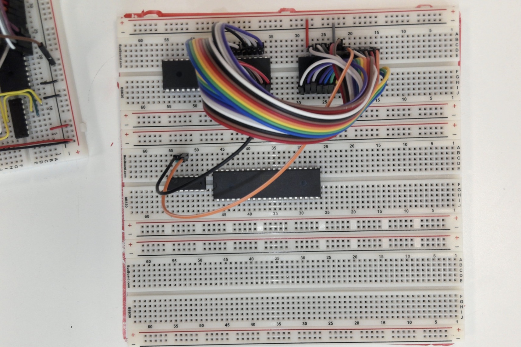
Connect all ICs to the breadboards in the following arrangement. The top left is the 6502, top right is EEPROM, bottom left is NAND, and bottom right is the 6522.
Address Lines
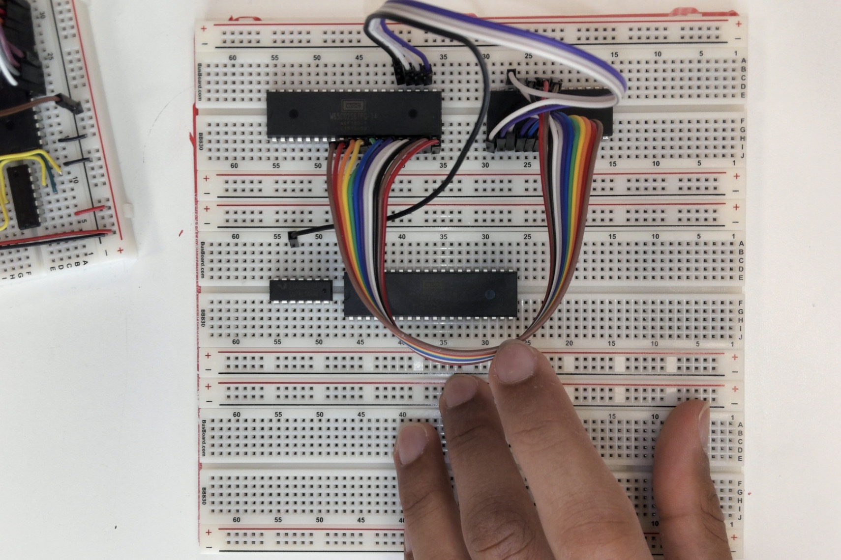
Connect the EEPROM to the 6502. Begin by connecting A0 from pin 9 on the 6502 to pin 10 on the EEPROM. Continue by connecting A1 from pin 10 on the 6502 to pin 9 on the EEPROM. Continue this pattern for all address lines from A1 to A14 by referencing the full schematic, looking at the leftmost IC (6502) and the second from the left (EEPROM).
Connect A15 to an input on the NAND chip.


Data Lines
Bridge the connection at the NAND chip to convert the NAND chip into an inverter for a single signal.
Complete the same process that you completed with the address lines with the data lines starting with D0 at pin 33 on the 6502 going to pin 11 on the EEPROM.


CS, OE, WE
Connect the output from the NAND chip to the CS pin on the EEPROM (pin 20) as seen with the orange wire. Connect OE to ground and connect WE to voltage.
Connect
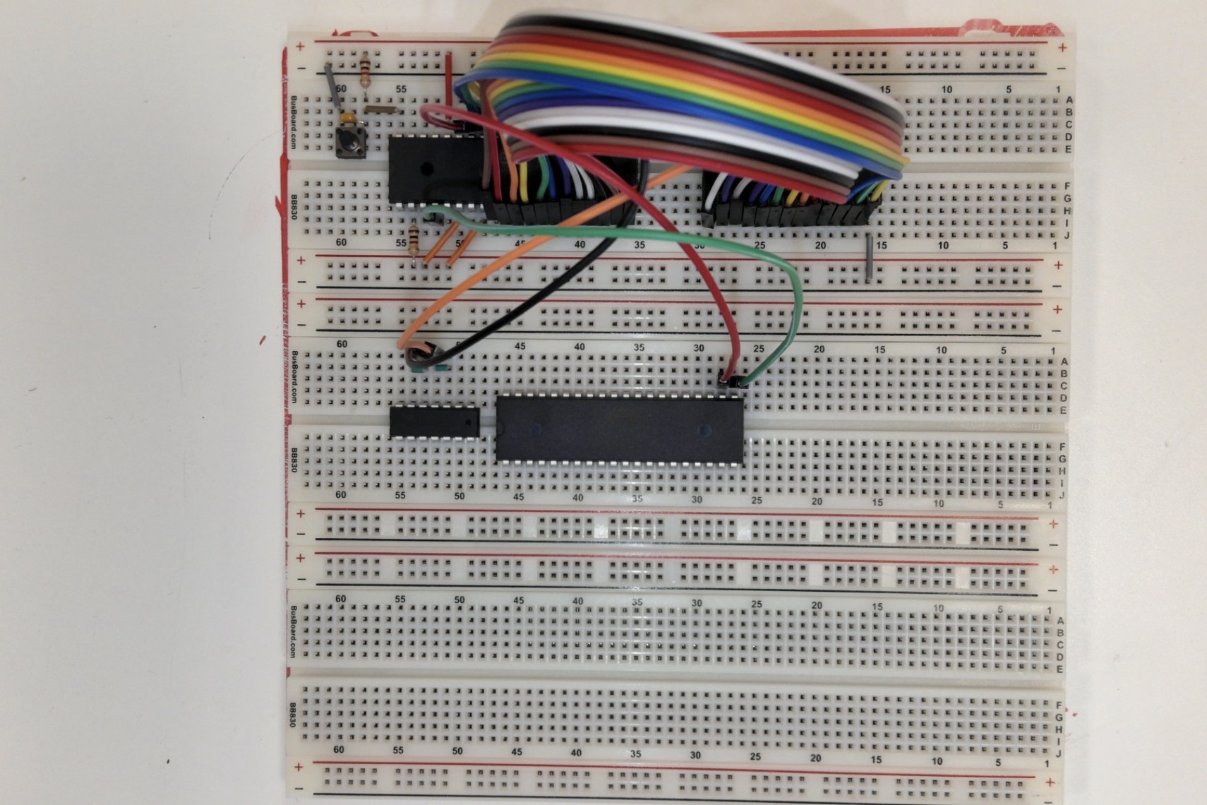
IRQ, etc.
Connect the IRQ pin on the 6502 (pin 4) to the corresponding pin on the 6522 (pin 21). Connect appropriate voltage and ground connections as pictured. The resistor used is a 1K resistor.
Also connect the output from the first NAND gate used to the input of the NAND gate next to the output with a small jumper. This will be used in a later step.


Reset
Connect the reset button as pictured. The resistor used is a 1K resistor.
Clock
Connect the clock as pictured. Ensure you orient the clock correctly. (Voltage in top right)
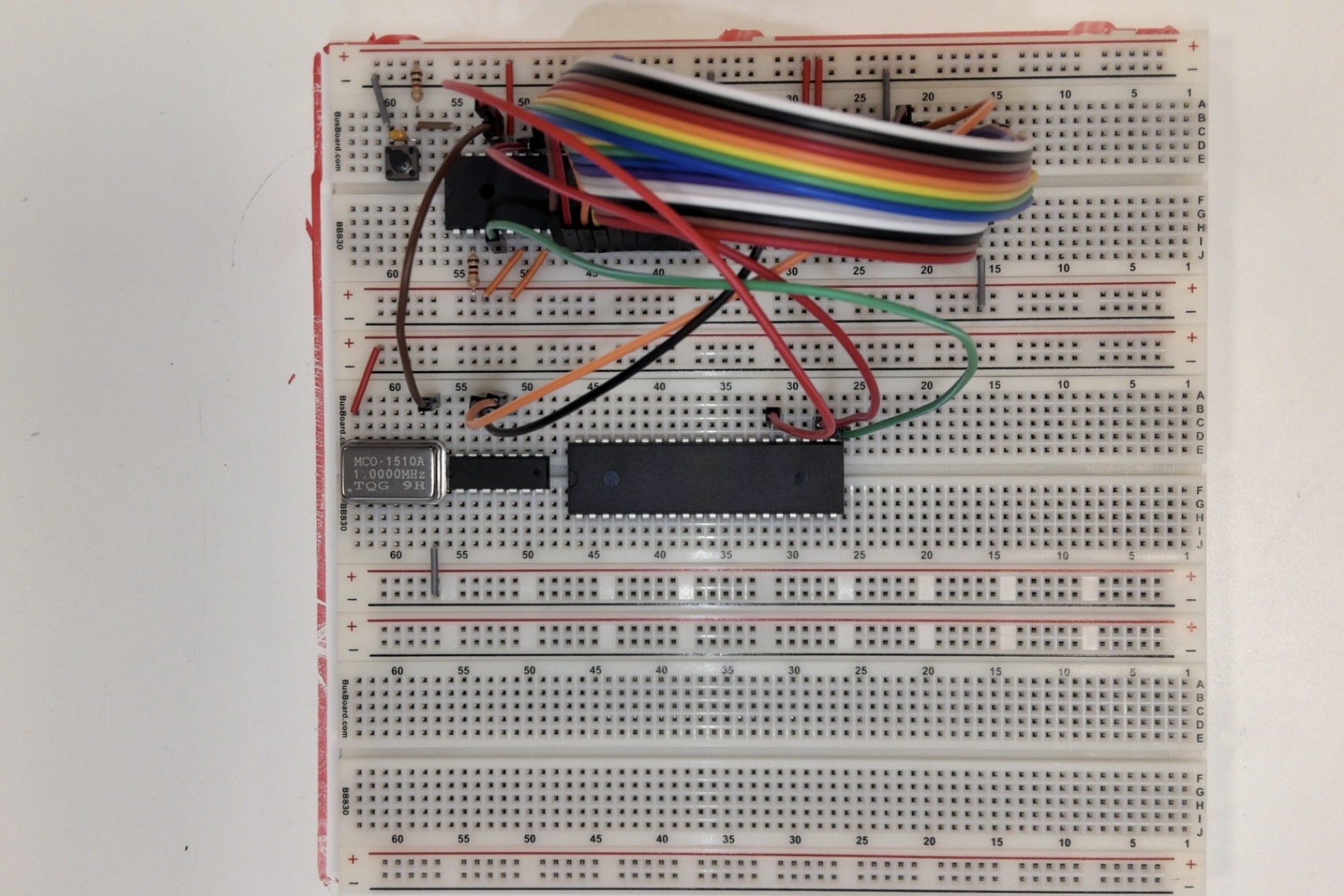
More NAND
Connect the clock to the NAND chip as pictured and connect all other connections from ther NAND chip to the NAND chip and from the NAND chip to the 6522.
The blue wire connected to pin 24 of the 6522 connects to A13 on the 6502 (pin 23).

Resistors
Connect 1K resistors to pins 2-6 of the 6522. Connect pin 1 to ground.
Screen!!!
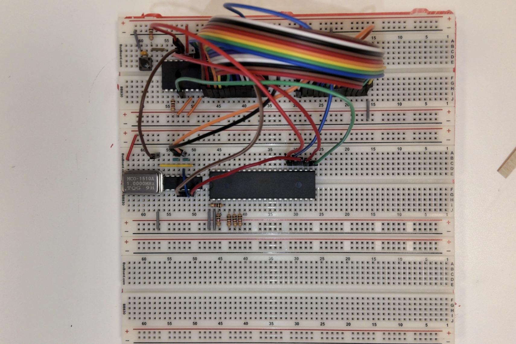
Connect Screen
Connect PB0-PB7 on the 6522 to DB0-DB7 on the screen. To begin, connect PB0 to DB0 by connecting pin 10 on the 6502 to pin 7 on the screen. Continue connecting 1-7 referencing the schematic for exact pinouts.
EEPROM to 6522
Connect the data lines from the EEPROM to the 6522.
Power
Connect the power rails.